Re-spinning a board is not a fun thing to do. However, it’s an important step to take and learn from our mistakes to improve the next revision of the board.
If you’d rather see an abridged version of this blog post, head on over to our Instagram page post here!
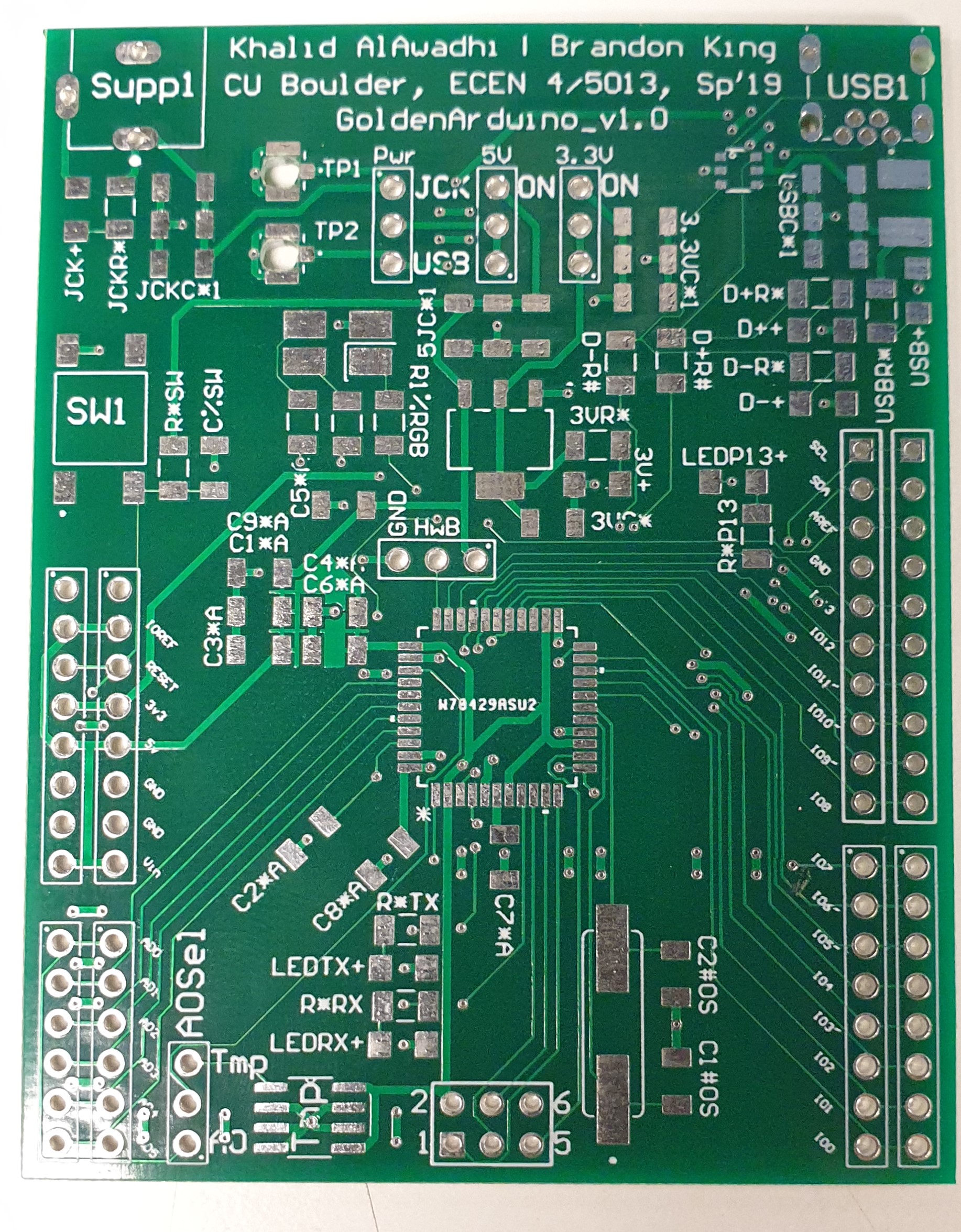
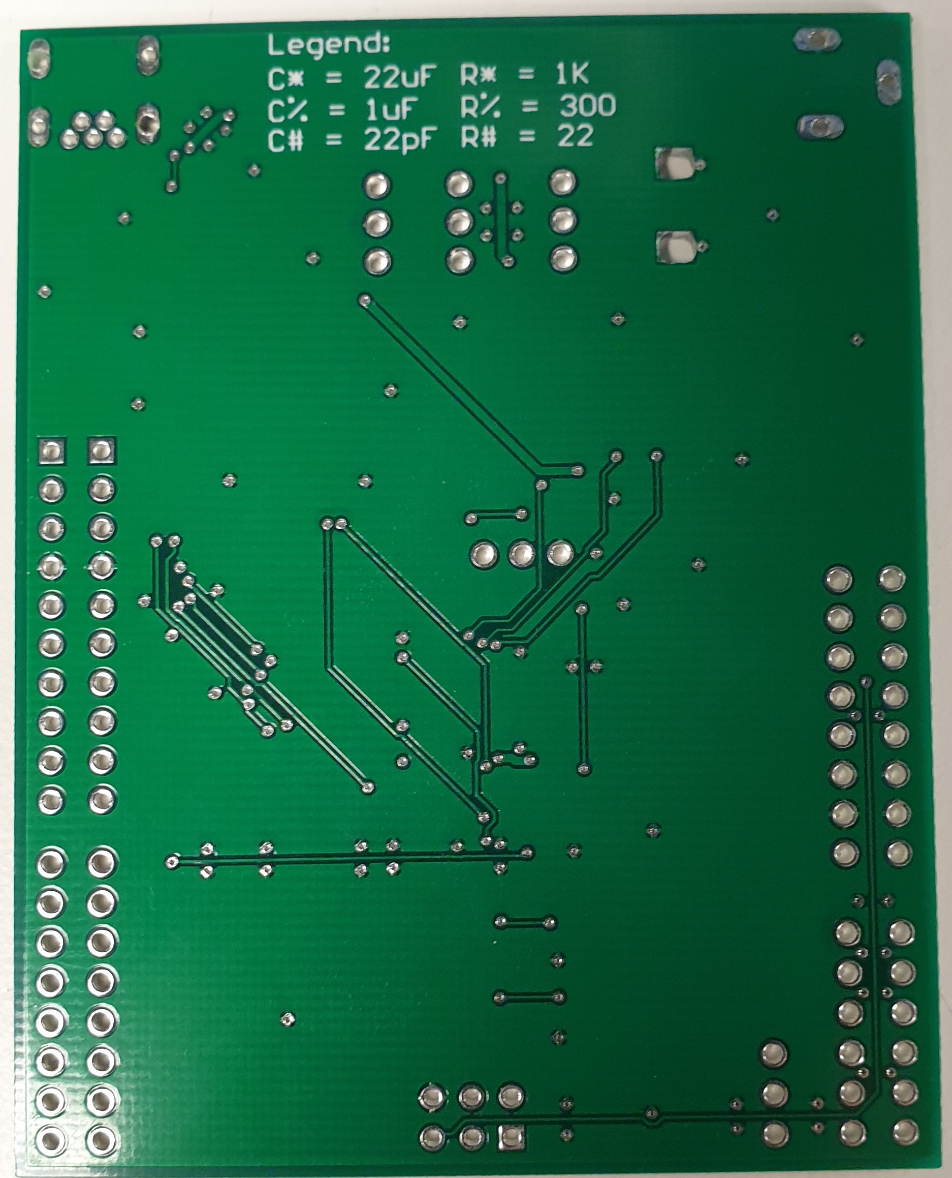
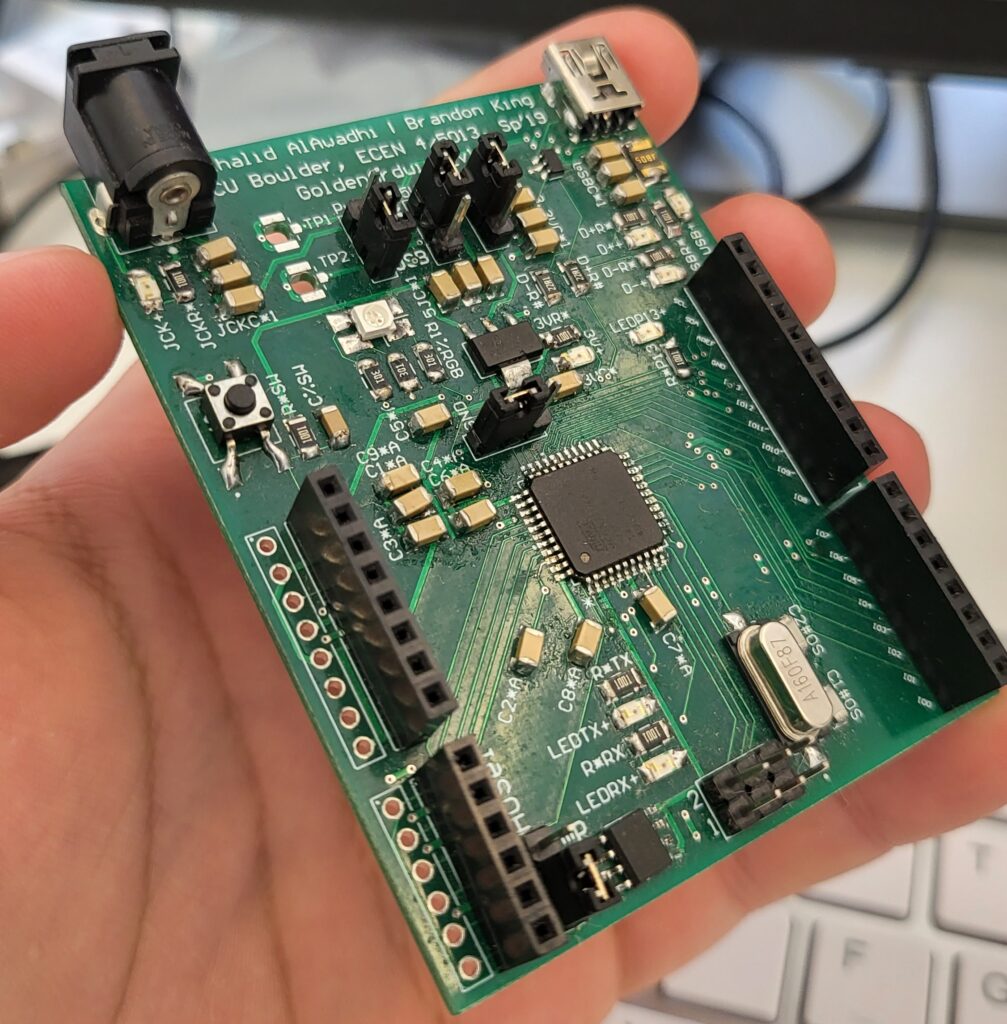
The first PCB I worked on was during college. We had to design an Arduino-compatible board. The professor called it the “Golden” Arduino board. By following some PCB design best practices, we made a board that is better than the commercial Arduino Leonardo board in terms of signal noise, power distribution, and mechanical integrity. I will probably cover those best practices in a future post. The golden Arduino board worked, but that design had some flaws.
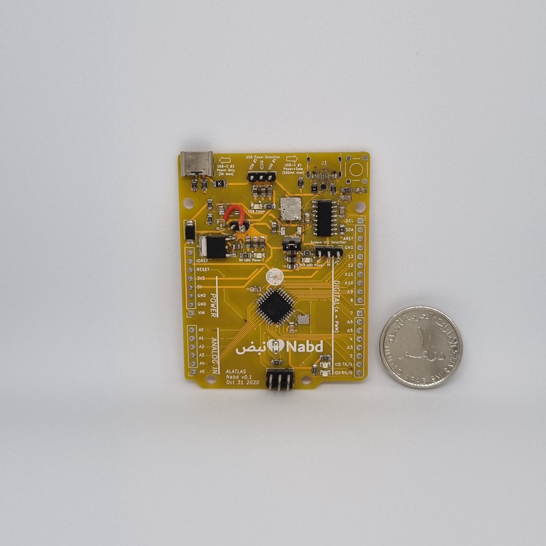
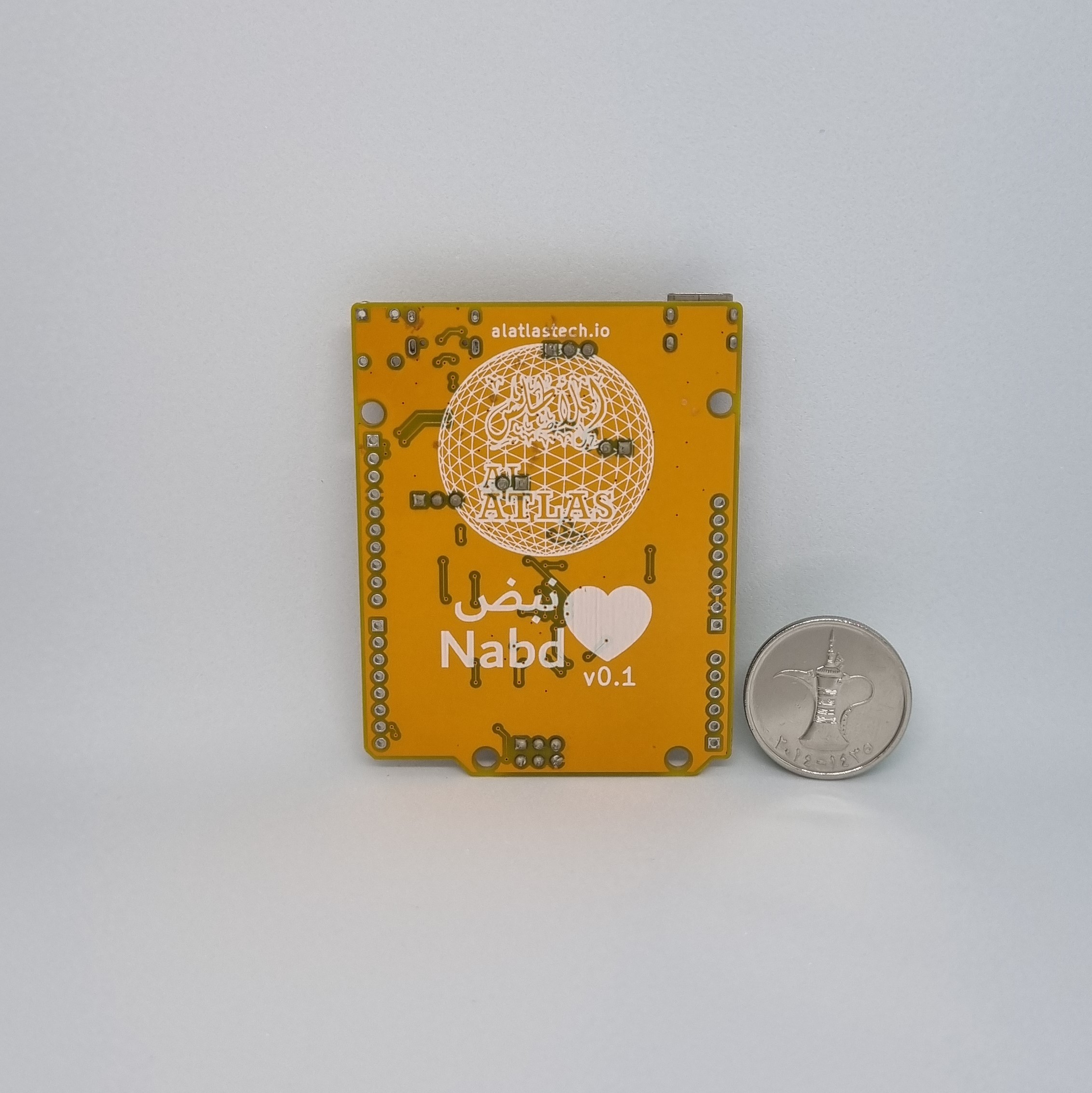
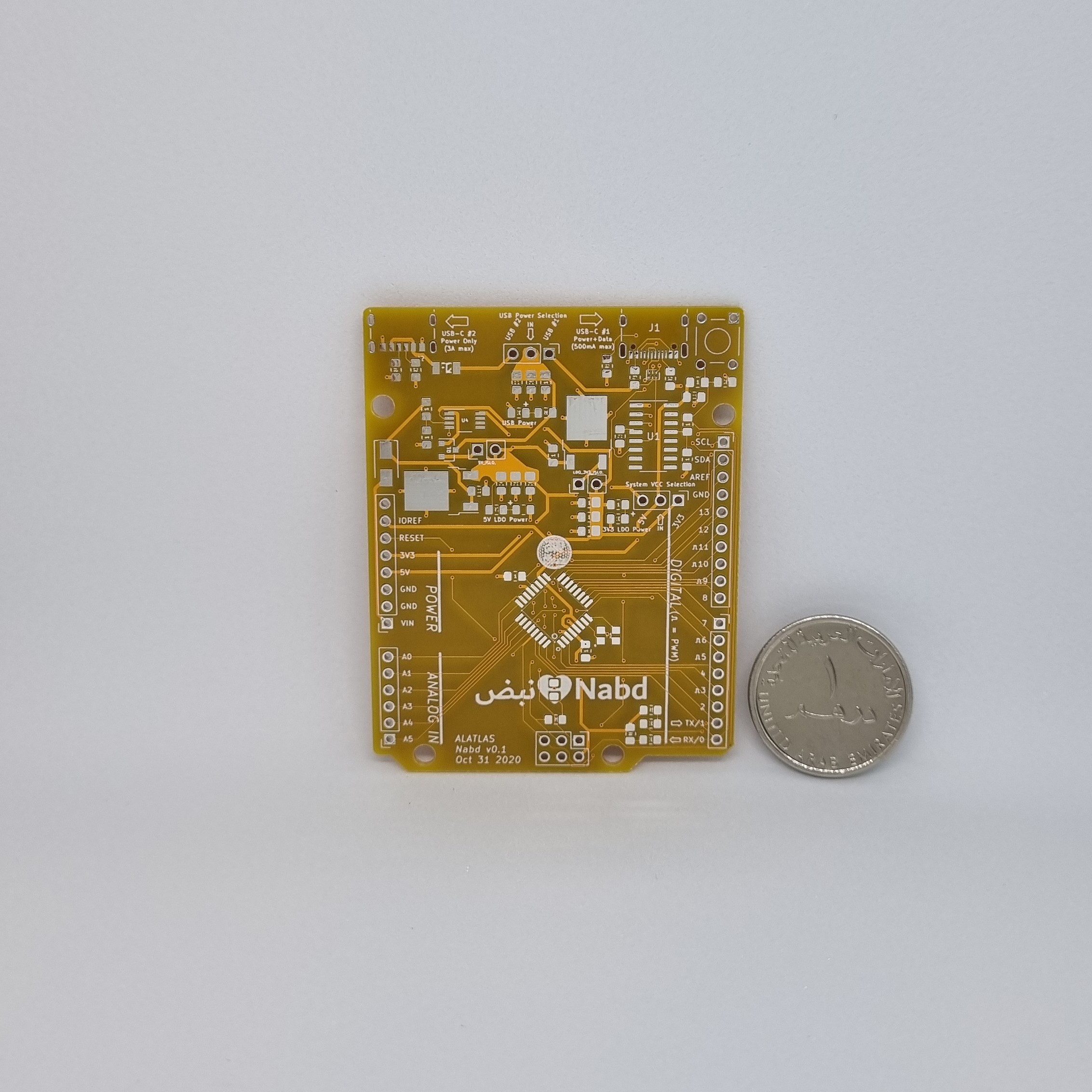
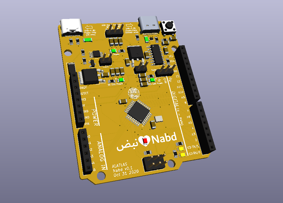
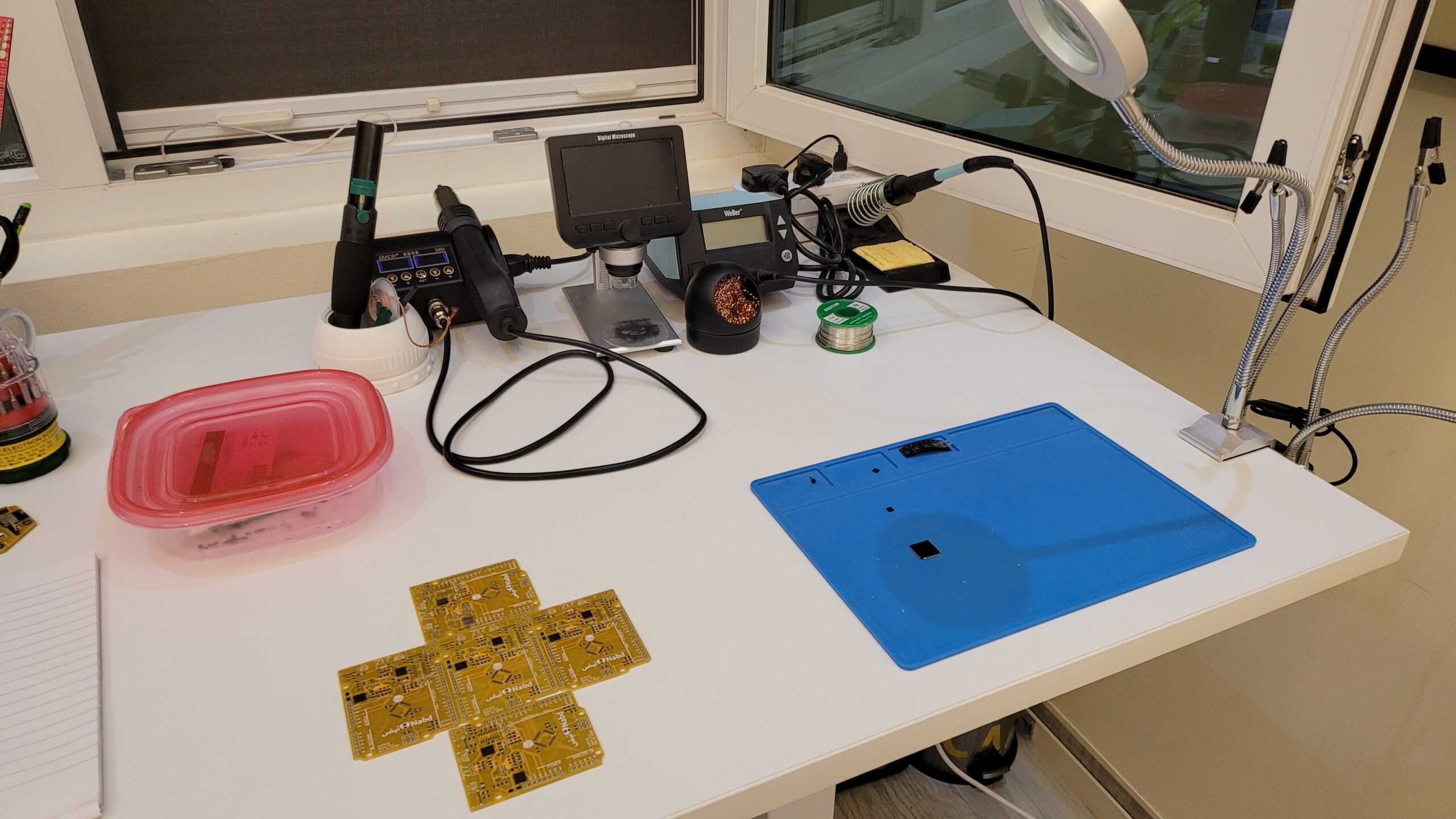
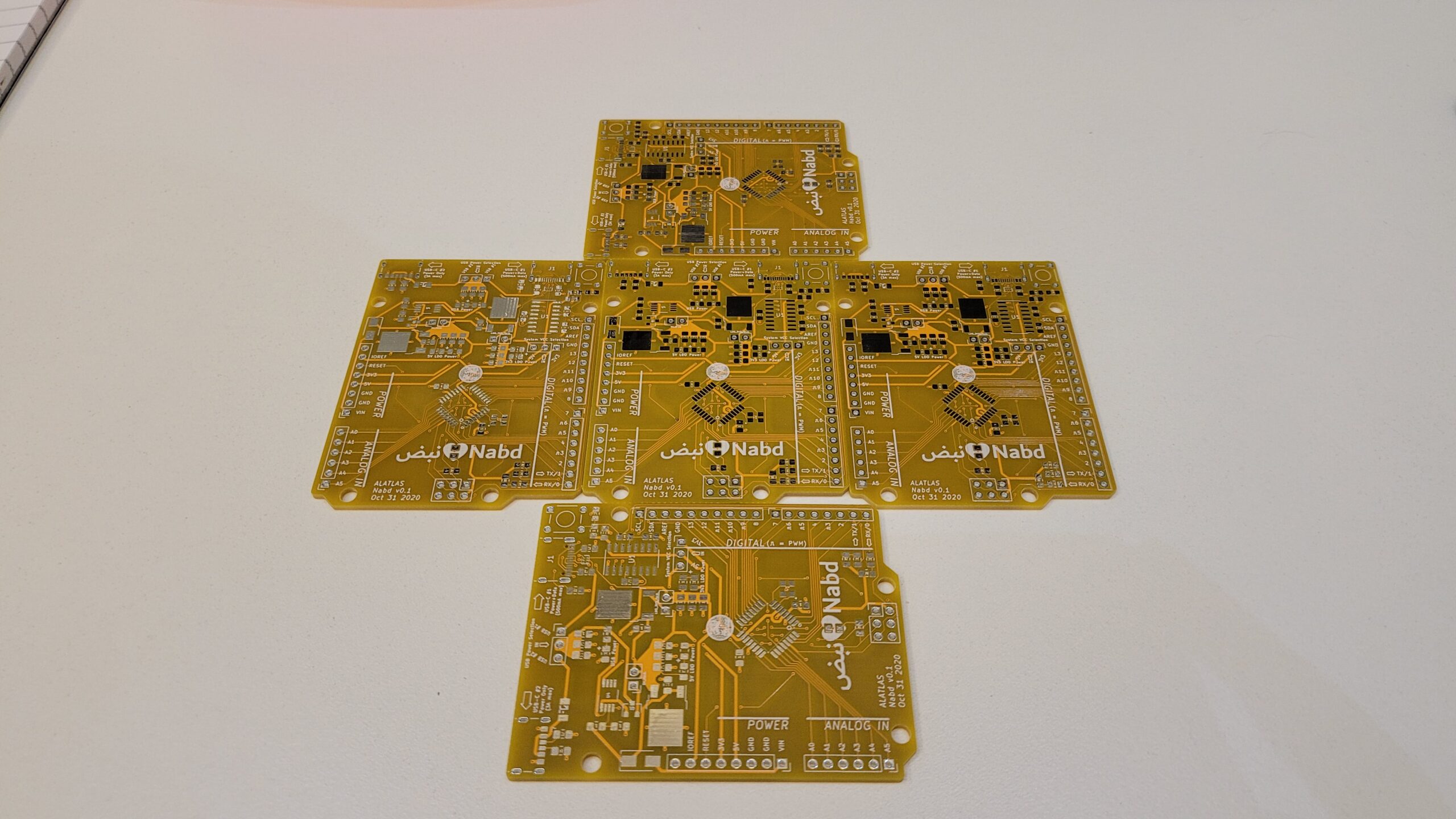
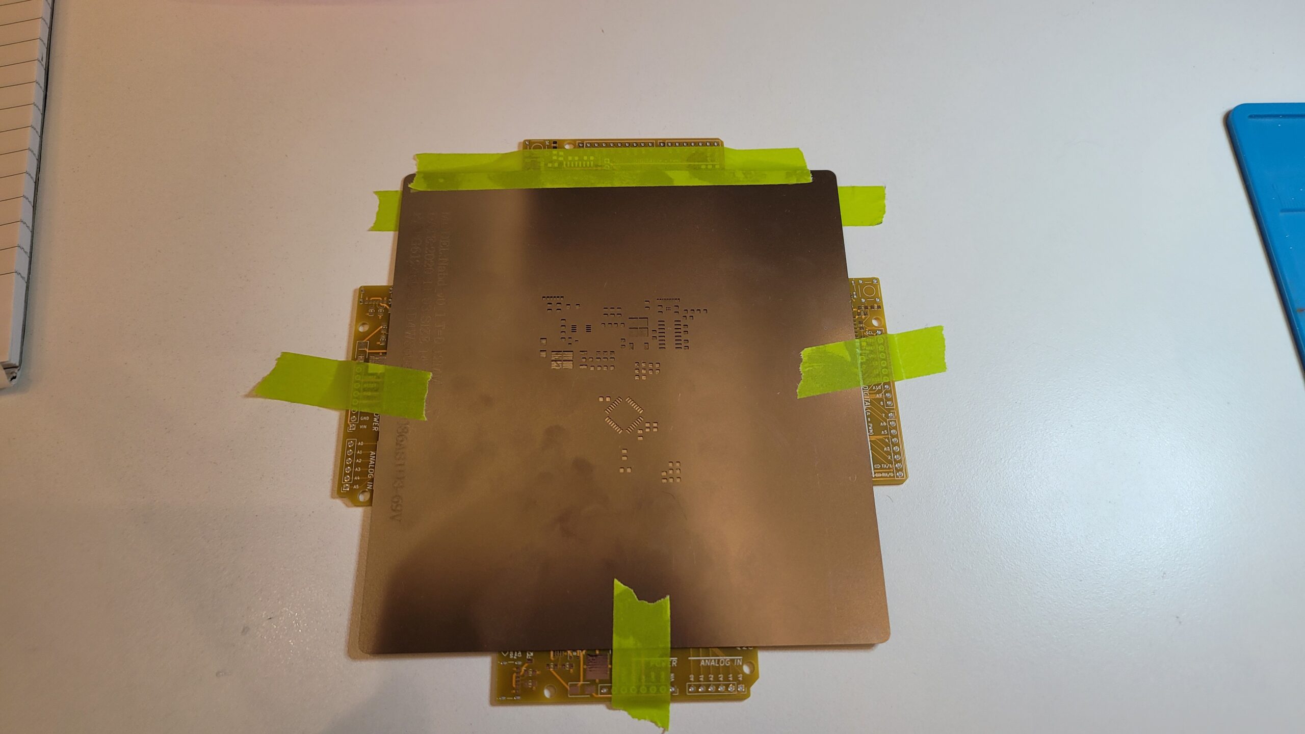
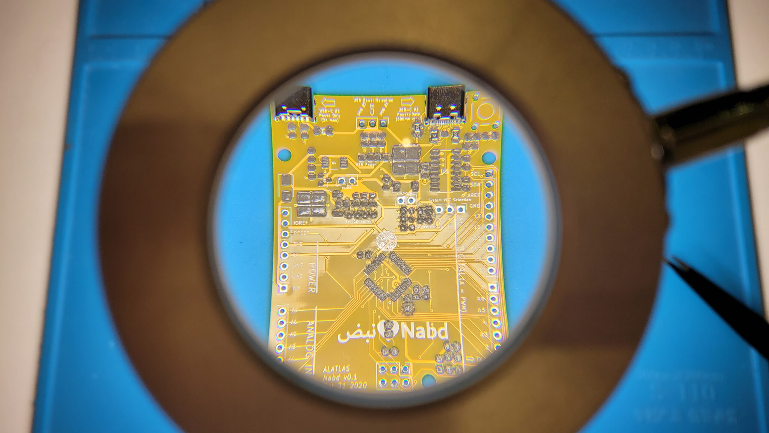
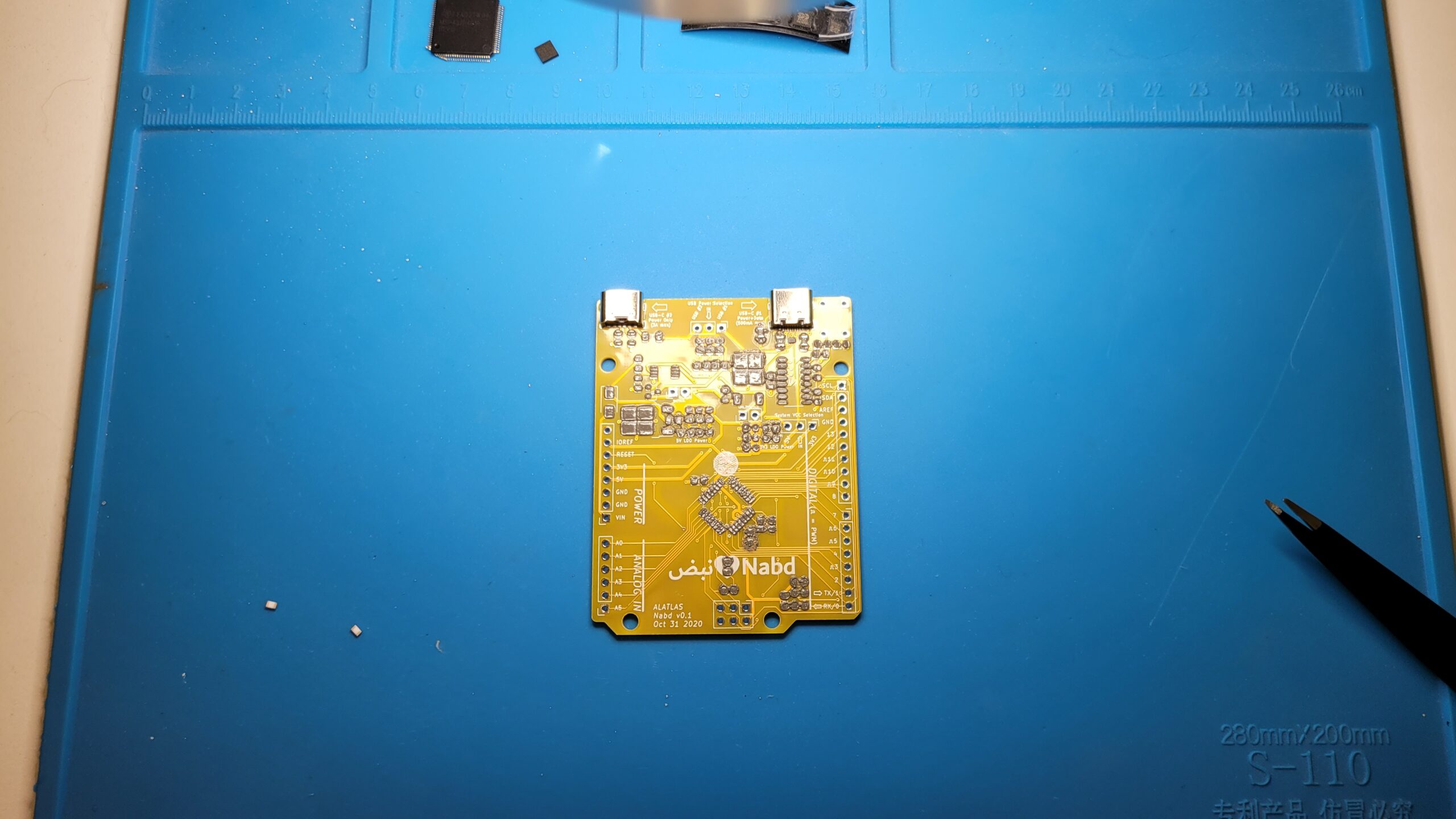
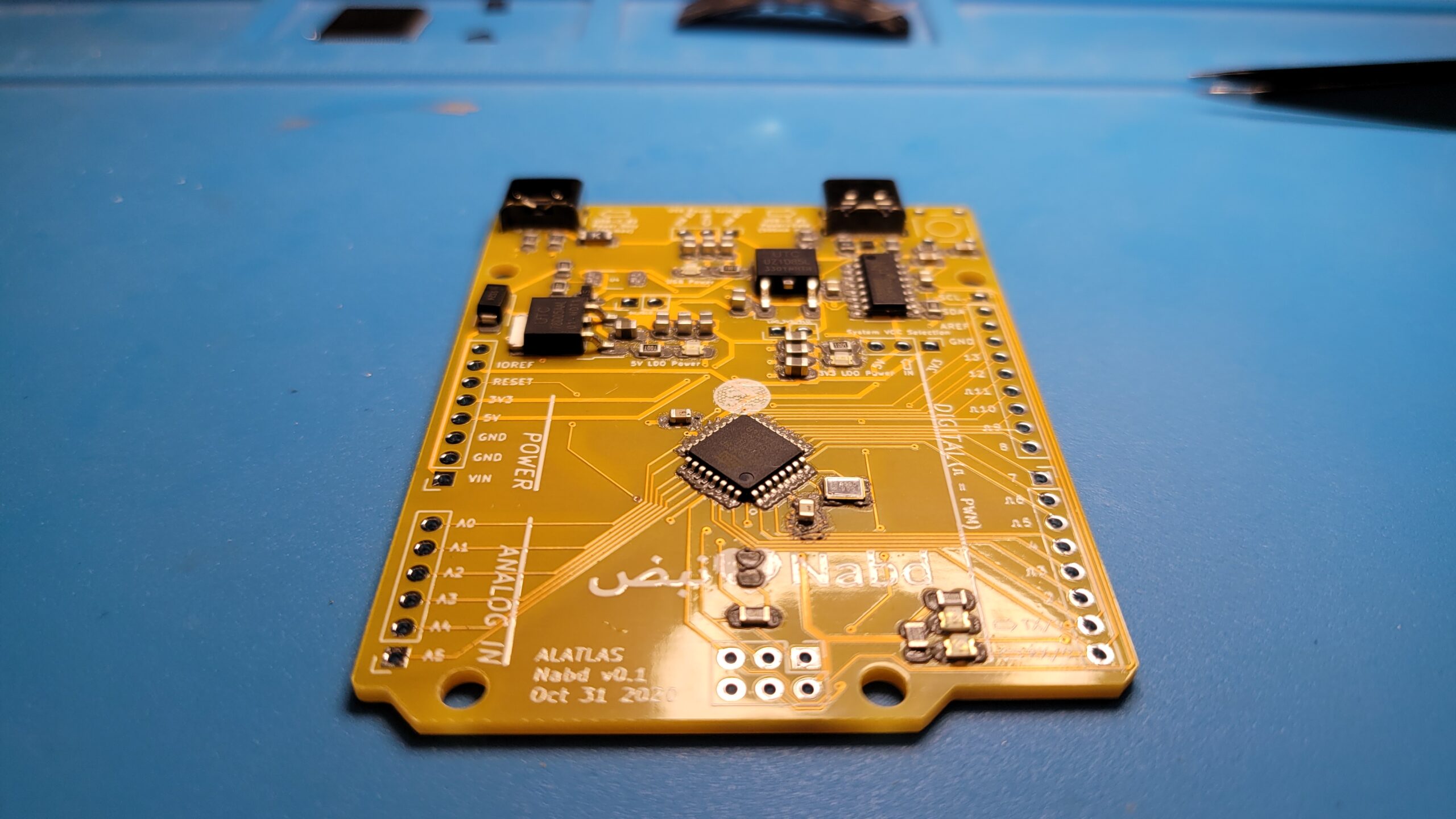
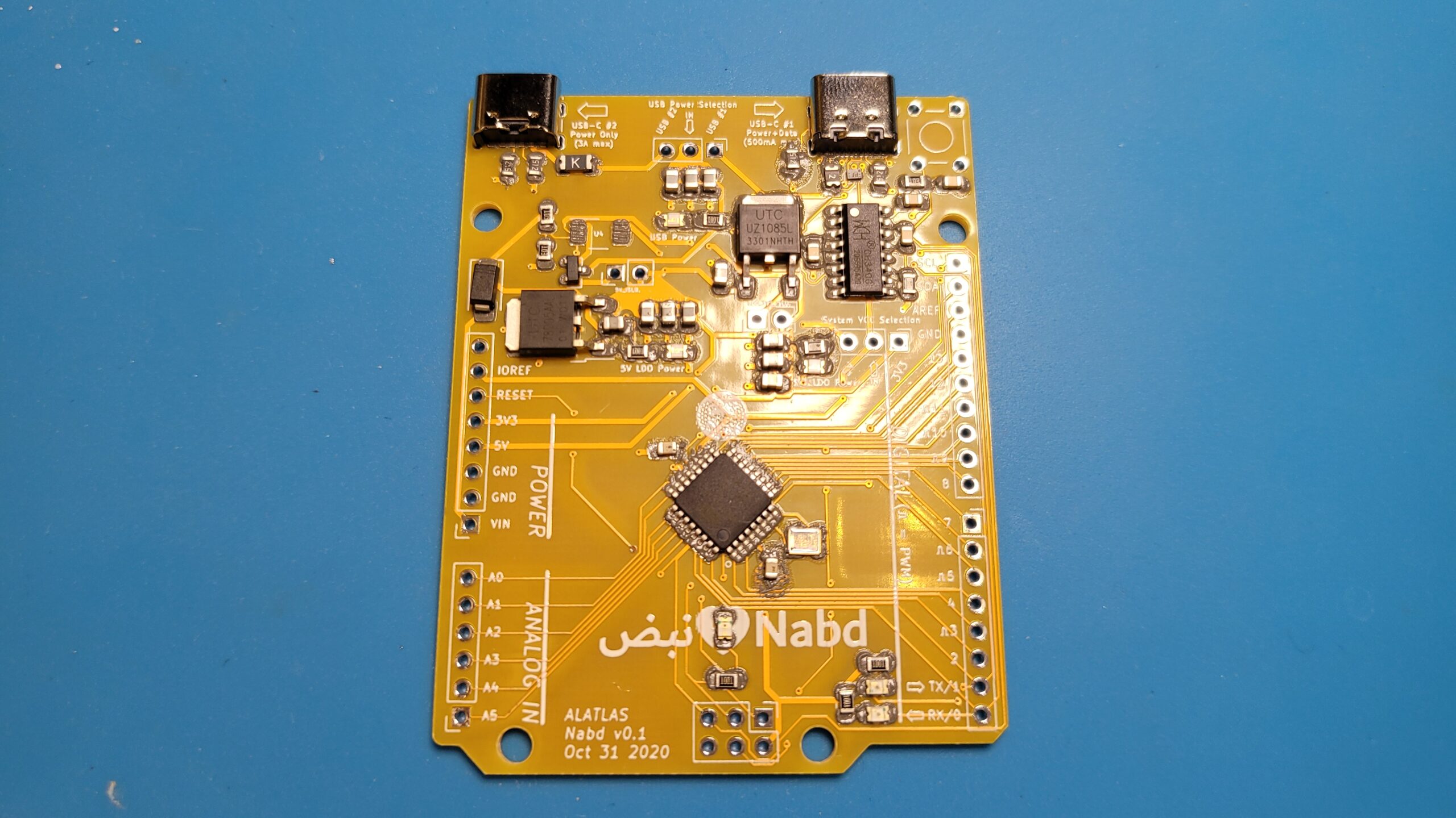
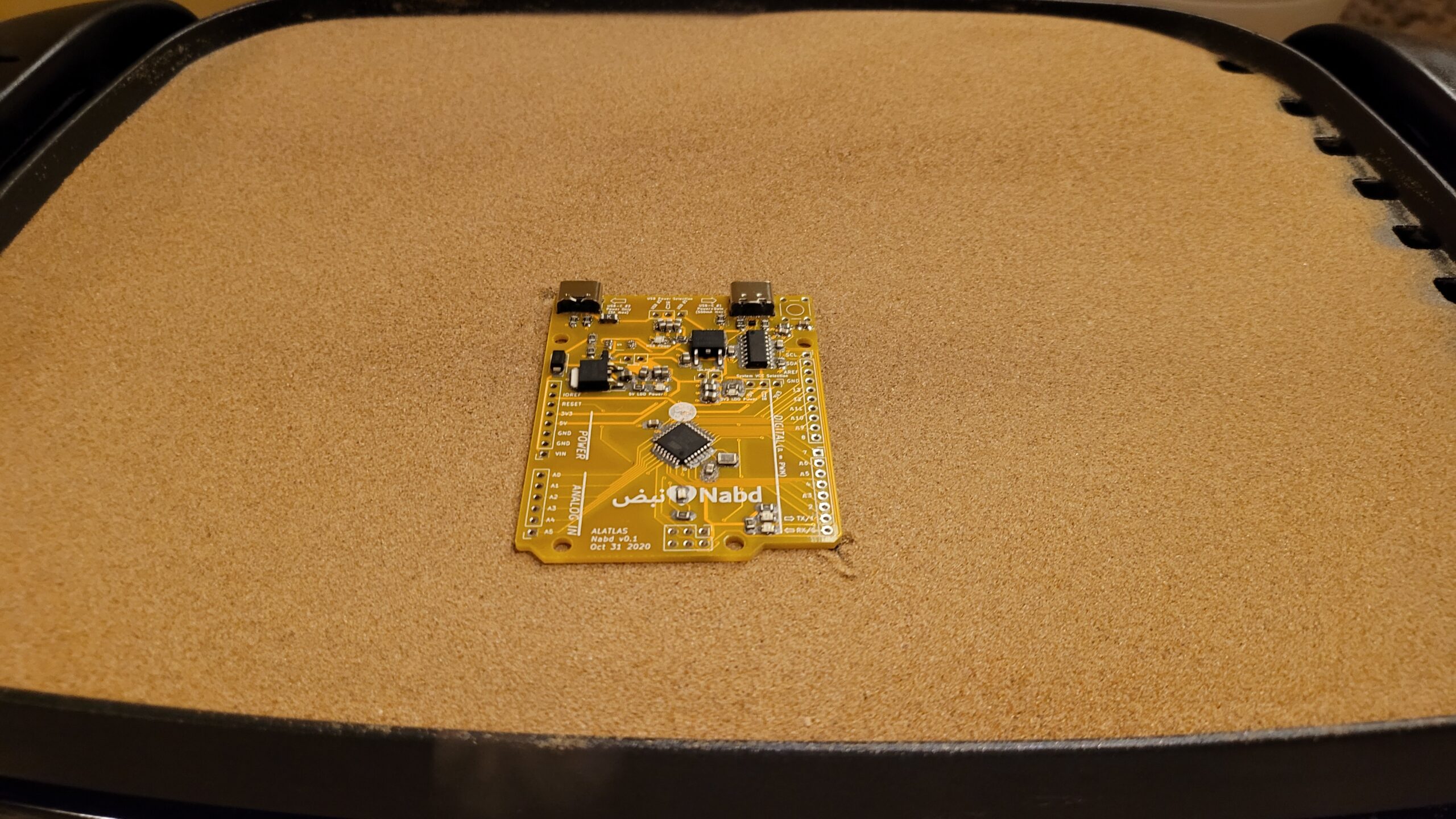
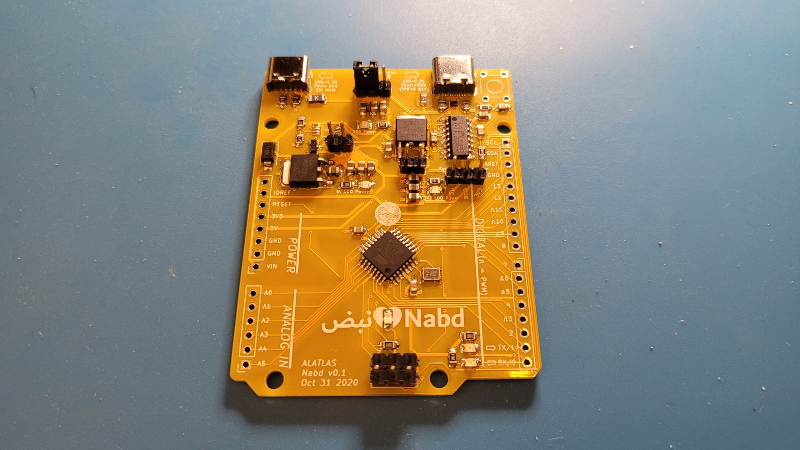
Nabd v0.1 was my second attempt at designing an Arduino-compatible board, with the Arduino Uno’s layout in mind to keep it compatible with shields.
Let’s dive in. Here are the major pitfalls I faced:
#1- Keep an eye out for islands when using a copper pour
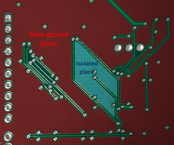
I know the title says why Nabd v0.1 failed, but a design flaw in my “Golden” Arduino board is worth mentioning. An island (or isolated copper pour) was in the ground plane.
For 2-layer PCBs, I always use the top layer for signal routing and the bottom layer for ground. Using the bottom layer as ground helps reduce electrical noise and interference, plus shortens signal return paths, which in turn reduces cross-talk.
When you route a signal from the top layer to the bottom layer, you essentially cut through the ground plane. That is usually fine as long as the distance in the bottom layer is kept as short as possible. However, if you don’t pay enough attention, you might accidentally cut the bottom layer enough to isolate a region and make it an island, as shown below:
The area in blue is what we call an “island.” It is electrically isolated from its intended copper pour plane. This is why you must be cautious when routing in the ground plane. The issue with an island is obvious: you have two areas that are not actually connected. You might still think they’re both ground; however, electrically they are not. Things will not work.
I am sure some of you are already planning to tell me that PCB design programs usually have an option to remove isolated copper pours, display a warning or something similar. I was just starting to learn PCB design and Altium in those days and didn’t even know about islands.
My partner and I didn’t have enough time to re-spin the board. The solution was to scratch both ground planes, exposing the copper underneath and then soldering a wire between them. Hacky, but it worked!
Despite that flaw, I used the golden Arduino for a couple of years until I made Nabd. It worked like a champ! You might notice other design flaws, those are covered in the following points.
#2- Mistaking IC packages
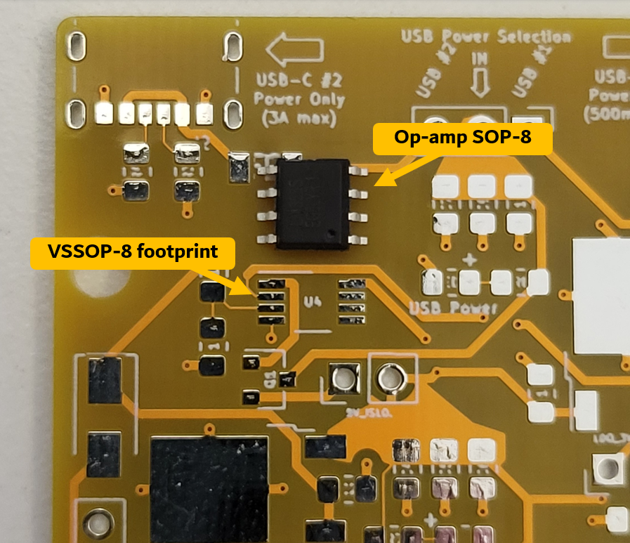
A common issue when designing PCBs is using the incorrect package footprint. This is what happened to the op-amp I used in Nabd v0.1. Classic.
I always have 3D models for my parts and double-check the model with the footprint it’s placed on. That is, if the model is made to be accurate for a specific footprint.
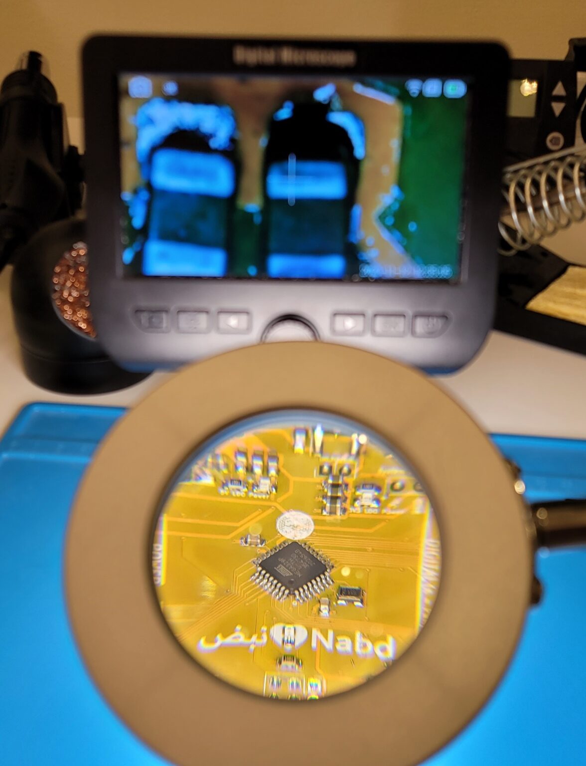
It turns out when I got the board, I misread and placed a different footprint than the actual IC I own. I chose a package footprint of VSSOP-8 (Very Thin Shrink Small Outline Package – 8 pins) when the op-amp I have is SOP-8 (Small Outline Package – 8 pins):
Because of that, I could not test the automatic power switching circuitry.
#3- Don’t trust symbols and footprints you find online, always double check
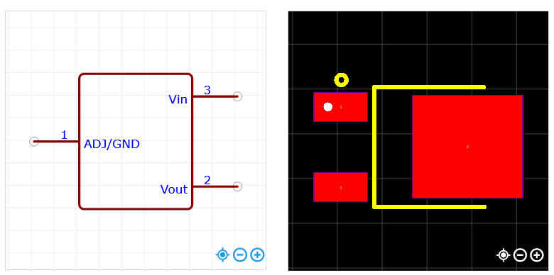
I made the error of trusting a symbol and footprint I found online. It looked reasonable and had the same footprint dimensions. It was the footprint of a standard TO-252 package (also known as DPAK). That footprint was for an LDO (low-dropout regulator).
Thought “hey, this looks good enough.” Therefore, I followed the same pinout shown on the symbol. Keep in mind that I had two LDOs with that same footprint, both from the same manufacturer. The only difference was that one outputs 3.3 volts while the other outputs 5 volts. The website showed me a very similar pinout for both, which looked something like this:
That symbol and footprint imply that the large area is GND (ground), and the other two pins are Vin (input voltage) and Vout (output voltage). So, I followed that in my design. Unless you look really closely, you’ll notice that the tiny numbers on the footprint do not align with how they’re shown on the symbol.
Next thing you know, when I was testing Nabd by applying some power, I saw the oh-so well-known magic smokebegin to rise from Nabd. Why? Specifically, the 3.3V LDO. Maybe a short I didn’t notice? I desoldered the LDO and resoldered a new one. Again, up in smoke. What’s happening?
I knew it had to be something with the LDO. Why was it overheating then cooking itself? I got another LDO and began testing on a breadboard. Following the pinout that was shown online, I noticed the LDO quickly overheats. I then tried changing the locations of Vin, GND, and Vout. I kept measuring Vout using an oscilloscope until I reached a combination that made the LDO work properly.
I then went to the manufacturer’s datasheet, and here’s the kicker – it turns out the pinout I used for the 3.3V LDO is wrong. The 5V LDO, however, had the correct pinout. Both look the same and are from the same manufacturer, yet they both have different pins for Vin, GND, and Vout.
I learned the hard way to always double check and don’t assume that because a symbol looks a certain way that the footprint follows it no matter how simple. I try to design my symbols to align with the footprint if it is a standard package and not complex. It helps you visualize how you’ll eventually place it in layout. Always double-check any new parts you receive! Thankfully, I was able to keep on testing Nabd v0.1 as it works with either 5V or 3.3V, so a missing 3.3V LDO wasn’t a showstopper.
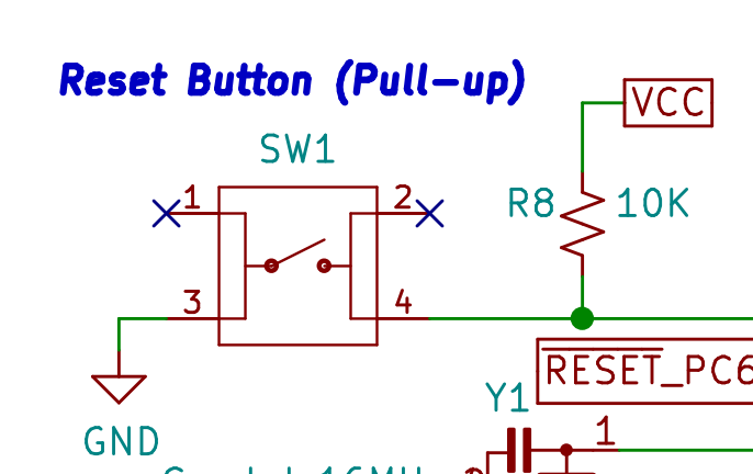
#4- Correct footprint, wrong pinout on symbol
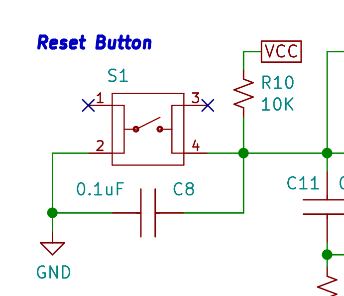
In a similar vein was the reset button. A very simple yet critical error. I connected pins on the board that were already connected to each other in the button itself. Basically, pointless.
Wrong: pins 2 and 4 are already connected physically in the button
Correct: Updated pinout of symbol to match button
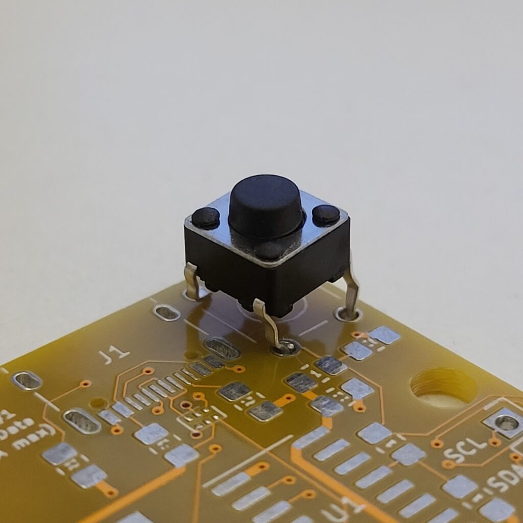
A quick fix was to rotate the button 90 degrees. I tested it and yup, that worked:
Temporary workaround. Didn't fit in place but hey, it worked
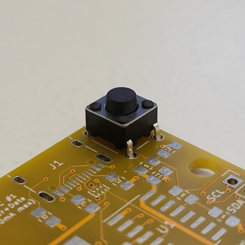
How the button should have been placed
It did not look good, but it was still workable for testing purposes. If you’re using a new component for the first time, double check your symbol pinout and footprint. You could’ve missed something!
#5- Make sure to choose component sizes you're comfortable working with
When selecting parts for any of your PCB designs, you must consider the package sizes of those parts. With smaller parts, you can pack more in a given area, but you’ll find it very difficult to pick and place by hand or hand solder if needed. The opposite is true for larger parts, which will leave you with less space but are easier to handle and hand solder. I made this mistake twice. Once in Shabakah v0.1 and again in Nabd v0.1. I finally learned my lesson.
In Shabakah v0.1, I used a tiny resonator, and it was a pain to align properly on its pad. Just look at how tiny this thing is! It’s almost the size of a grain of sand:
Technology is amazing. But it was a nightmare to handle and place properly.
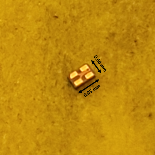
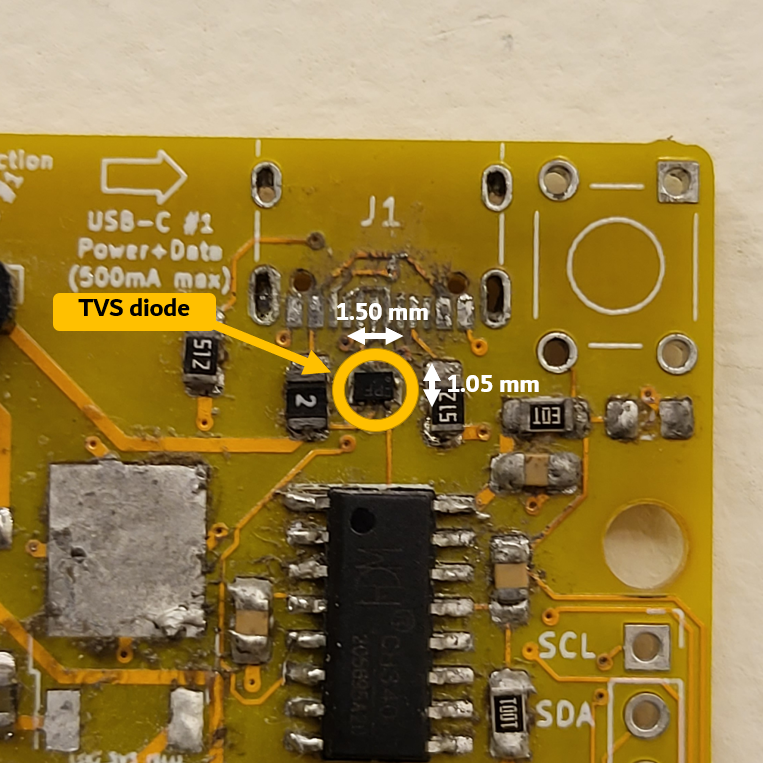
As for Nabd v0.1, I chose a tiny TVS (transient-voltage-suppression) diode, thinking it’s not as small as the resonator, so it won’t be that bad. Turns out, it was worse.
The tiny resonator only had four pads that needed to be aligned on the footprint. The TVS diode, on the other hand, while slightly larger, had six pads to be aligned. Any slight deviation or solder bridges and I’ll have to remove it and resolder:
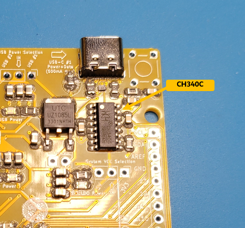
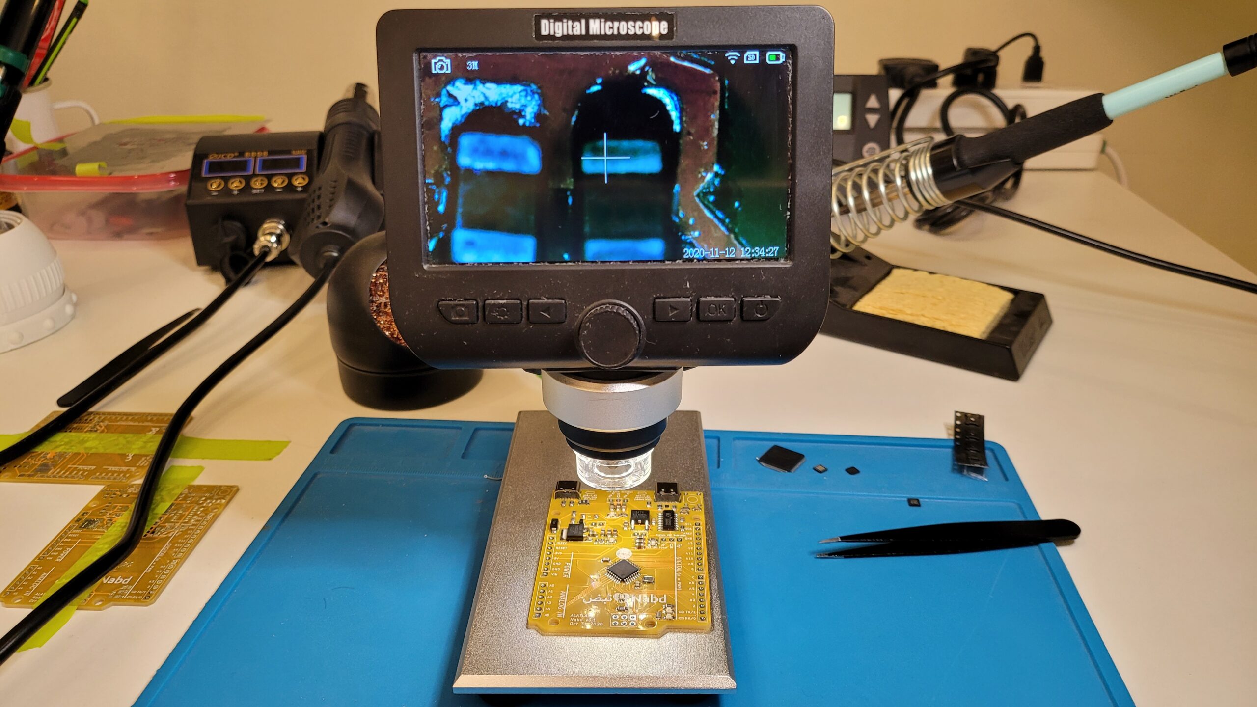
And oh boy, did that happen. As you can see from the wasteland in the above picture, I struggled a lot with Nabd v0.1. The PC wouldn’t recognize the board as being connected. Was it bad USB-C connections? An issue with my PC? Was the MCU faulty? A bad CH340C IC (used to convert USB to serial UART)? So many factors were in play, and it took me hours to figure it out. I eventually found out it was all the TVS diode’s fault; it simply wasn’t soldered properly. I had to remove and resolder it multiple times until the USB-C port worked.
For Nabd v2, I completely removed the TVS diode and opted to believe in the manufacturers’ making those PCs safe! The TVS diode will probably be back, and it’s a good component to have. Maybe in Nabd v3?
#6- Research the ports you are going to use before adding them
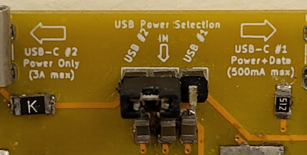
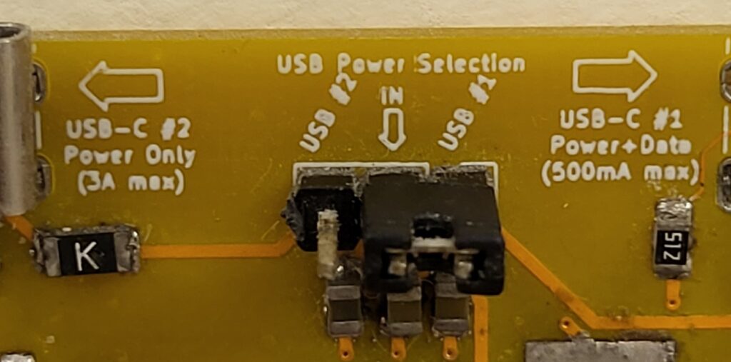
I initially wanted a design that would incorporate two USB-C ports. Why two? Because I thought I’d make one power only, providing up to 3A of current. And the other focused on data handling, capped at 500mA. The user could switch between the two sources that power Nabd v0.1 via jumpers:
Power from 3A port
Power from 500mA port
While this works, in hindsight, it doesn’t make sense. I’ll be honest, I really didn’t think it through. It seemed like a good idea initially, but when Nabd v0.1 arrived, I realized this was redundant. Why not simply use one USB-C port that is both capable of handling data and providing 3A of current?
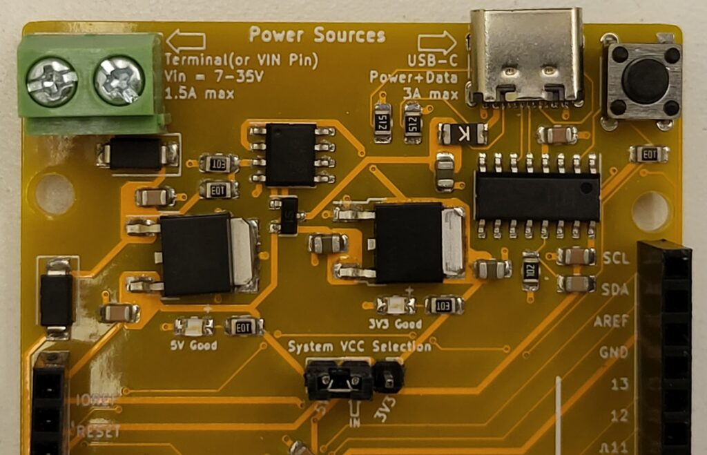
I was new to the USB-C standard, and I’m still learning. I assumed having a possible power draw of 3A without a proper fuse might damage the host PC. However, according to the USB standard, host PCs will already limit current based on what they can provide. Two different USB-C ports were not needed or efficient. That understanding allowed me to replace the power-only USB-C port with a screw terminal on Nabd v2, which is much more versatile:
Nabd v2 updated ports
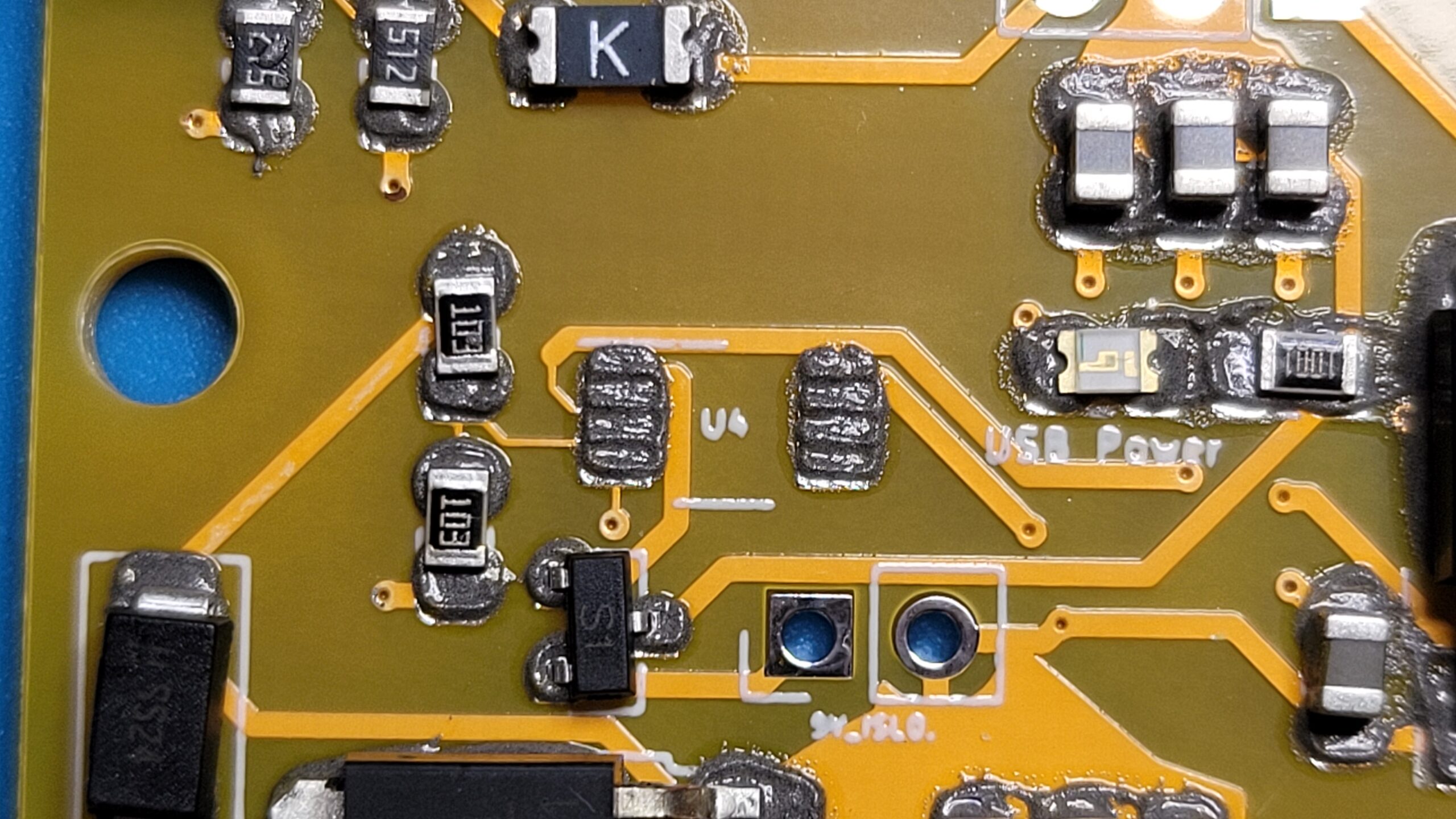
#7- Capacitor interference on sensitive lines
Although this point might be very specific to certain use-cases, I will mention it anyway. I always add debouncing circuitry to any buttons I place. You could do it in software, but I highly recommend doing the debouncing in hardware if you can. It’s a simple yet robust addition.
In my Nabd v0.1 design, I use the CH340C IC to handle converting USB to serial UART, which allows easy code uploading to Nabd via the Arduino IDE:
To keep it brief, the CH340C required a capacitor of a certain value to connect between it and the reset pin of the MCU. On that same line is the physical reset button, which I added a debouncing capacitor to.
When the time came to upload code to Nabd v0.1, I couldn’t get it to work. And of course, it took me a while to debug this issue. Again, a lot of factors were at play. After extensive debugging and testing, it turned out the CH340C could not reset the Nabd, which was necessary to enter the bootloader and allow code to be uploaded.
The solution was simple: remove the debounce capacitor placed on the same line and only keep the needed capacitor for the CH340C. That allowed CH340C to reset Nabd when needed.
In hindsight, it makes sense. I added more capacitance without considering if it’d have an impact. The additional debounce capacitor interfered with the CH340C’s ability to communicate with Nabd’s MCU and upload code.
The debouncing circuitry at the reset button is not critical and was only done as a form of good practice. Overall, it wasn’t a bad compromise.
Final thoughts
Working on Nabd v0.1 was not easy, but I sure learned a lot! Nabd v2 was much easier to assemble, test, and bring-up. Making mistakes will only improve your craft if you do not insist on them, of course, so keep trying!
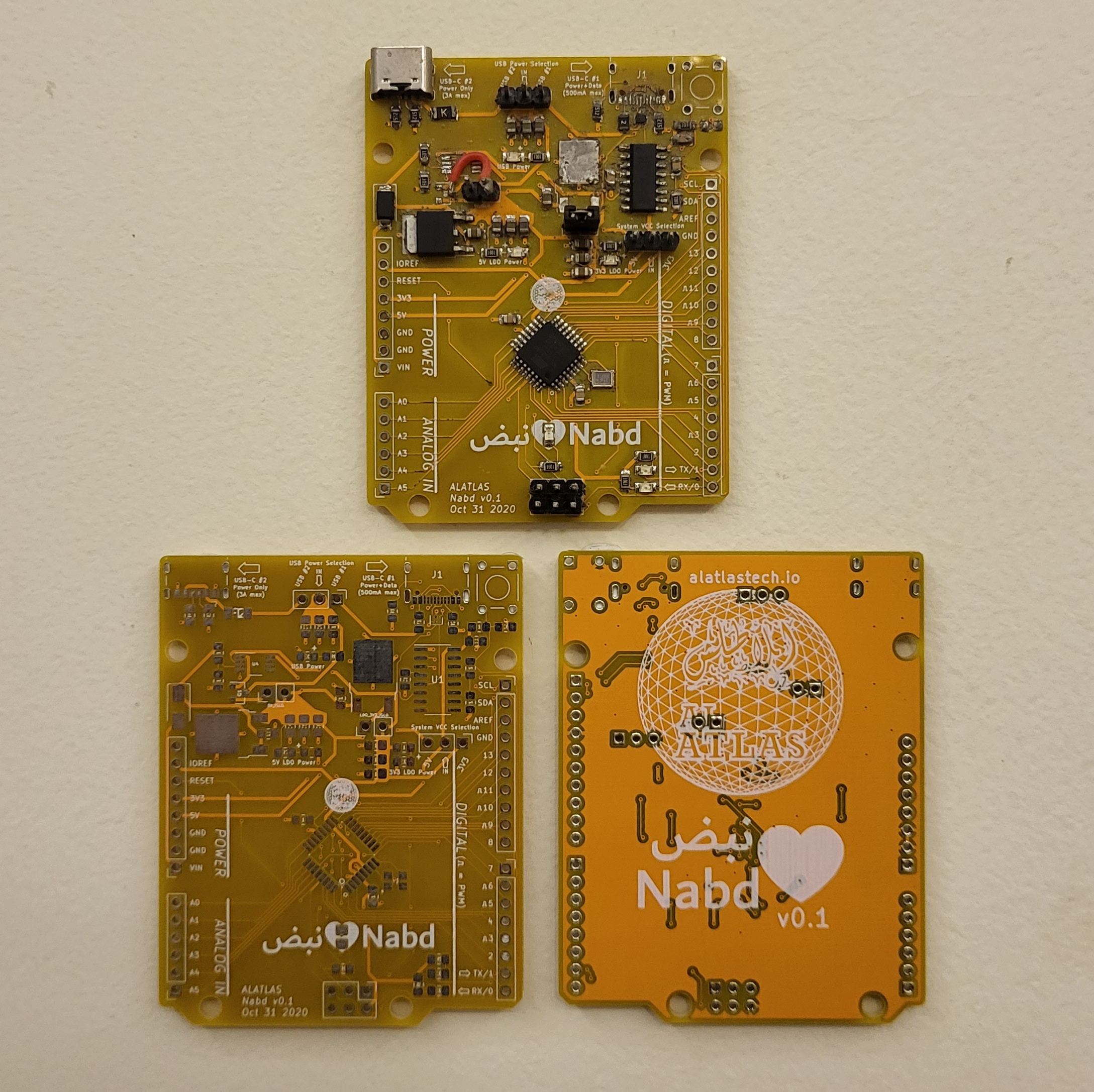
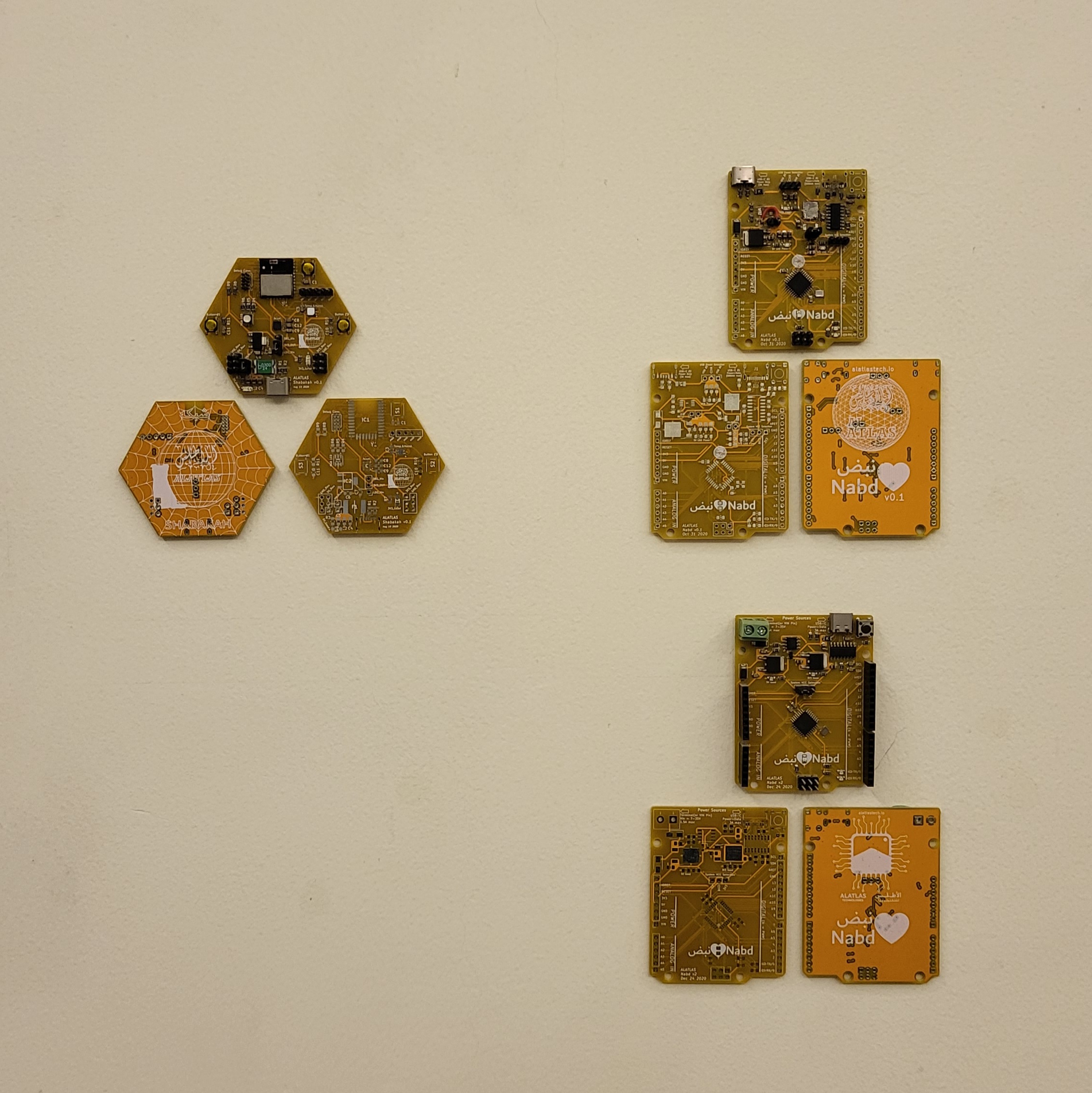
Only one semi-assembled Nabd v0.1 remains, and it hangs on my wall, along with other Remal boards, as a monument of trial, error, learning, and improvement:
Those, in short, were some of my PCB design pitfalls which I personally experienced. Hopefully, you’ll be able to avoid them in your future designs. Keep building and failing; it’s a great way to learn. Or you could have someone with more experience take a look before you place a PCB order!
Got any other pitfalls or something to keep in mind when working on PCBs? Share them below!